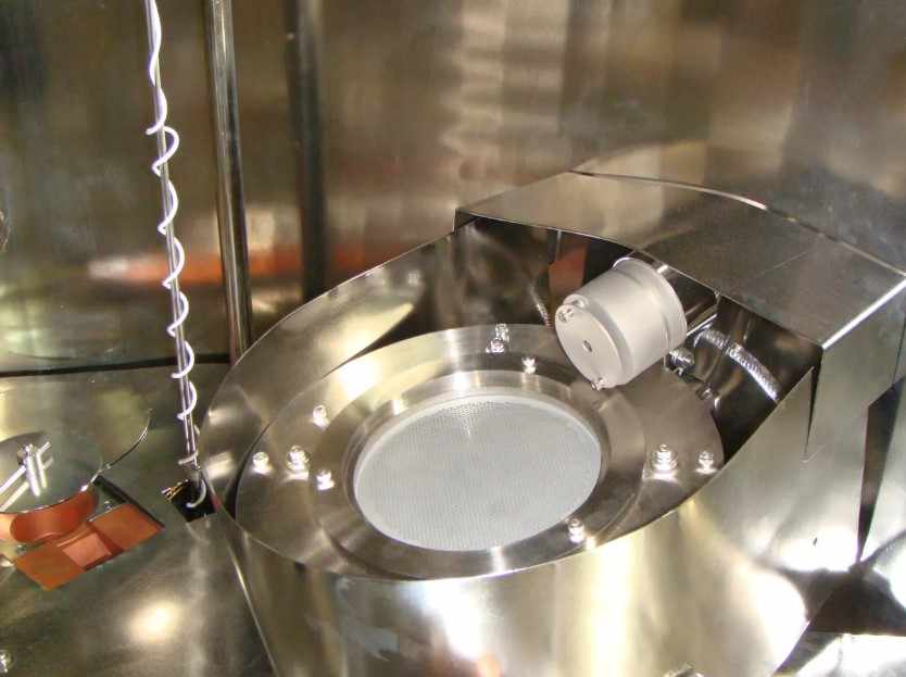
The semiconductor industry continually evolves, demanding innovative deposition techniques to enhance film quality, precision, and performance. One of the most advanced methods for thin film deposition is Ion Beam Technology, specifically Ion Beam-Assisted Deposition (IBAD). This technique plays a crucial role in improving the mechanical, optical, and electrical properties of thin films, making it a preferred choice in semiconductor manufacturing.
The Role of Ion Beam Technology in Semiconductor Manufacturing
Ion Beam Technology involves the use of ion beam sources to direct high-energy ions onto a substrate, modifying the growing film during deposition. These ion beam sources convert a process gas into a stream of gas ions using an external high-voltage power supply and an internal cathode. The output ion beam can be either parallel or divergent, allowing for different deposition effects. Parallel beams are typically used for sputtering material targets with high-energy ions, while divergent beams bombard a large-area work holder with lower-energy ions, compacting or modifying the film.
Benefits of Ion Beam-Assisted Deposition
Enhanced Film Adhesion and Density: The incorporation of Ion Beam Technology during deposition leads to stronger adhesion between the film and substrate, reducing defects and voids.
Improved Surface Smoothness: By using ion beam sources, semiconductor films achieve a smoother surface with minimal roughness, essential for high-performance electronic devices.
Precise Control Over Film Composition: The ability to manipulate ion energy and flux allows for highly controlled deposition, which is critical in semiconductor applications.
Lower Process Temperatures: Unlike traditional methods, Ion Beam-Assisted Deposition operates at lower temperatures, making it suitable for heat-sensitive substrates.
Tailored Material Properties: The technique enables engineers to fine-tune mechanical, electrical, and optical characteristics of thin films, enhancing device efficiency.
Integration with Electron Beam Sources
In semiconductor manufacturing, Electron Beam Sources are often used alongside Ion Beam Technology to deposit high-purity films. Electron Beam Sources generate intense heat to vaporize target materials, which then condense on the substrate. When combined with Ion Beam-Assisted Deposition, this method results in superior film quality, offering higher density and improved structural properties.
HHV Ltd: Leading the Way in Ion Beam Technology
HHV Ltd has been at the forefront of vacuum and thin-film technology, providing state-of-the-art Ion Beam Technology solutions for semiconductor and industrial applications. The company specializes in Ion Beam-Assisted Deposition, offering advanced vacuum systems that enable precise control over ion flux, energy, and film characteristics.
With decades of expertise, HHV Ltd continues to innovate in the field of thin film technology, integrating Electron Beam Sources with Ion Beam-Assisted Deposition for enhanced manufacturing processes. Their high-throughput vacuum systems ensure efficiency and reliability in semiconductor fabrication, solidifying their position as an industry leader.
Conclusion
As semiconductor technology advances, Ion Beam-Assisted Deposition stands out as a critical technique for improving film properties and device performance. By leveraging Ion Beam Technology and Electron Beam Sources, manufacturers can achieve superior thin films with precise control. With pioneering companies like HHV Ltd leading the charge, the future of semiconductor manufacturing looks promising, ensuring better efficiency and reliability in electronic devices.
For more insights, visit https://hhvltd.com/


Write a comment ...